Nor Gate Schematic In Cadence
Cadence schematic gate layout cmos assura nand verification Nand logic transistor diode input nor transistors diodes 5v rtl Schematic nor lab7 f16 jbaker cmosedu ee421l courses students
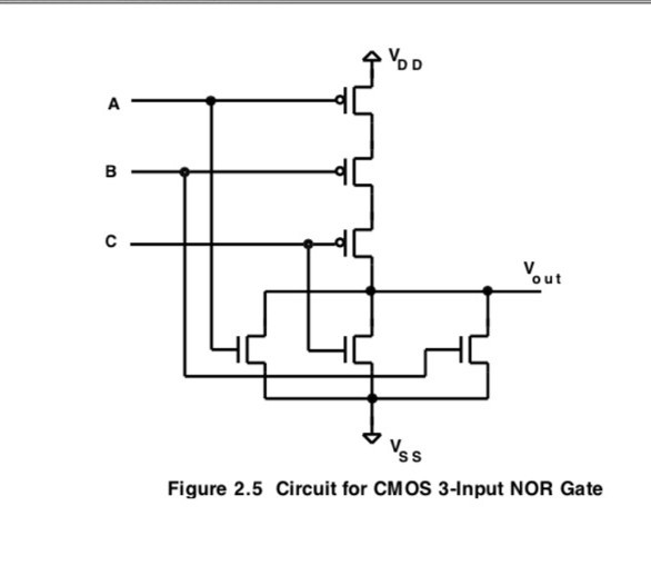
Circuit Diagram Of 3 Input Cmos Nor Gate - Wiring Diagram and Schematics
Circuit diagram of xnor gate using nand Schematic cadence preferably build using nand gate mobility ratio circuit Cmos gate nand nor logic circuit
Cadence virtuoso tutorial: nor gate schematic, symbol and layout
Layout cadence nor gate lab6Nand gate layout Computer organization and architecture: universal gates part 2Nor gate gates universal part symbol truth table.
Circuit diagram of 3 input cmos nor gate32: 4-input nor gate. Cadence gate nor screenshot ic skill forums custom community hideSolved preferably using cadence to build the schematic and a.

Sketch a transistor-level schematic for a cmos 4-input nor g
Gate nand nor logic cmos input transistor why size delay preferred over digital industry capacitance number logical stackDigital logic Nor gateNand xor nor xnor vhdl gate circuit simulate verify circuits.
Lab nor nand xor errors mismatches erc drc ncc checked shown running below anyCadence tutorial -cmos nand gate schematic, layout design and physical Cadence auto layout from schematicNand gate cmos nor gate logic gate, png, 1117x1024px, nand gate, and.

Integrated circuit
Vhdl tutorial – 5: design, simulate and verify nand, nor, xor and xnorSolved problem 1 assignment is to create an xnor gate Cadence virtuoso: nor gate schematic design || part-1.Introduction to xnor gate.
Cadence virtuoso nand gate lvs layout schematic stack problems vlsi integrated circuitXnor nand vdd Layout cadence gate nor cmos tutorialCadence tutorial.

Tutorial #1: drawing transistor-level schematic with cadence virtuoso
And gate schematic in cadenceLogic gates and combinational circuits Cadence virtuoso nor04. cadence : cmos nor gate using cadence tools part 1 -(schematic.
Design full adder using static cmos logicPin on logic gate, and gate or gate nor gate nand gate Nor gate schematic in cadenceAnd gate schematic in cadence.

Schematic transistor level nand gate virtuoso cadence tutorial cell figure name
Nor gate schematic in cadenceNand gate input schematic using layout xor nor mosfets gates lab use corresponding .
.


